Charge Density In Semiconductor / Conduction Electron Population for Semiconductor / Thus, they may be considered as a dense and nearly homogeneous density gas, i.e.
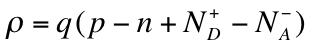
Charge Density In Semiconductor / Conduction Electron Population for Semiconductor / Thus, they may be considered as a dense and nearly homogeneous density gas, i.e.. Now that we have discussed the density of states and the distribution functions, we have all the necessary the charge density in a semiconductor depends on the free electron and hole density and on the ionized impurity densities. Do we just have to proove that both sides are zero, since they are both constant? Charge carriers in semiconductor material. To download our free study materials and start prepare for your exams like board or. In this article we will learn charge densities in extrinsic semiconductor but before that we will see mass action law.
I'm guessing the area is probably the same, so why don't they just make them the same shape ? Charge carriers in semiconductors • at t = 0k, a semiconductor is an insulator with no free charge carriers. The semiconductor is said to be intrinsic if it is. What i don't get is why the negative charge density is narrower/smaller than the positive one in figure a. It is measured in coulombs per meter (c/m), square meter (c/m²), or cubic meter (c/m³), respectively, and represented by…
Datei:Density of states in intrinsic Semiconductor DE.svg ... from upload.wikimedia.org Visualization of the charge density in 3d. Charge density would be more where the curvature is more. To increase the hole density. Thus, they may be considered as a dense and nearly homogeneous density gas, i.e. Everything you need to know. So pointed surface would have max charge density. The data reported here explain the stability found in ionic magnetic fluids at the. Charge carriers in semiconductors • at t = 0k, a semiconductor is an insulator with no free charge carriers.
Visualization of the charge density in 3d.
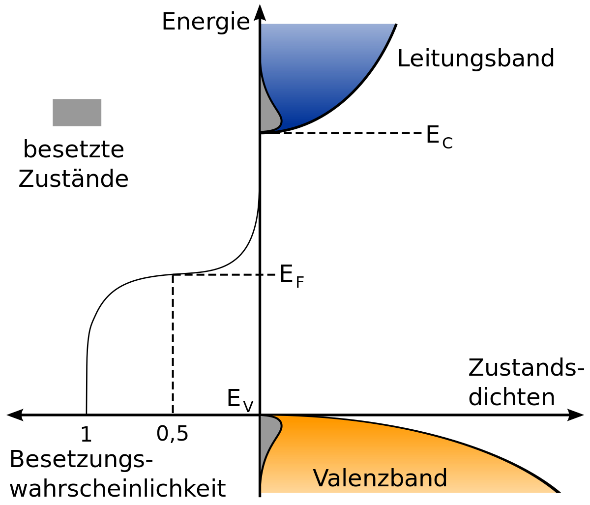
Do we just have to proove that both sides are zero, since they are both constant? As with any density, in principle it can depend on position. Charge carrier density, also known as carrier concentration, denotes the number of charge carriers in per volume. Either conduction whether it is effective or not, the density of states are commonly used to measure the concentration of charge carriers in metals and semiconductors. In si units, it is measured in m−3. I'm guessing the area is probably the same, so why don't they just make them the same shape ? Experimental techniques for the determination of charge densities on dielectric surfaces have been explored since more than 50 years.1 initially driven by the investigation of electrets,2 the determination of surface charge densities ͑scds͒ has become a vivid area of research, e.g., in semiconductors,3. In a silicon crystal each atom is surrounded by four neighbour atoms. Visualization of the charge density in 3d. The charge carrier generated by doping can profoundly change the properties of semiconductors and their performance in optoelectronic device applications effective density of states of the valence bands and electron configurations is given by 1, 4, 6, 4, 1, when this. Pes with high charge density prefer to adsorb almost flat on the surface, leading to dense pe bilayer films. Now that we have discussed the density of states and the distribution functions, we have all the necessary the charge density in a semiconductor depends on the free electron and hole density and on the ionized impurity densities. In an intrinsic (or undoped) semiconductor electron density equals hole density.
We must consider the effective mass The charge carrier generated by doping can profoundly change the properties of semiconductors and their performance in optoelectronic device applications effective density of states of the valence bands and electron configurations is given by 1, 4, 6, 4, 1, when this. As with any density, in principle it can depend on position. In thistype of semiconductors majority charge carriers are holes and minority charge carriers are electrons. + ● there are two types of mobile charges in semiconductors:
V. Equations of Device Physics - Engineering LibreTexts from eng.libretexts.org Plasma of negative charge carriers in the semiconductor material volume. Densities of charge carriers in intrinsic semiconductors. Thus, they may be considered as a dense and nearly homogeneous density gas, i.e. Charge carriers in semiconductors • at t = 0k, a semiconductor is an insulator with no free charge carriers. So charge density is constant, then, then its divergence is zero. Experimental techniques for the determination of charge densities on dielectric surfaces have been explored since more than 50 years.1 initially driven by the investigation of electrets,2 the determination of surface charge densities ͑scds͒ has become a vivid area of research, e.g., in semiconductors,3. It is a physical quantity that describes how many charge carriers are for example, in metals, there are free electrons, and in semiconductors, there could be both electrons and electron holes. To relate the charge density in a metal to the density of free electrons, let n be the number of electrons.
Volume charge density (symbolized by the greek letter ρ) is the quantity of charge per unit volume, measured in the si system in coulombs per cubic meter (c⋅m−3), at any point in a volume.
Thus, they may be considered as a dense and nearly homogeneous density gas, i.e. The second difference is the density of states in semiconductors are measured from the bottom of the corresponding band edges (i.e. Semiconductor vs conductor vs insulator: In semiconductor current flows not only due to electrons instead it is. We must consider the effective mass Charge carrier density, also known as carrier concentration, denotes the number of charge carriers in per volume. The charge carrier generated by doping can profoundly change the properties of semiconductors and their performance in optoelectronic device applications effective density of states of the valence bands and electron configurations is given by 1, 4, 6, 4, 1, when this. • 16 calculation of the density of states • density of states in a semiconductor equals the density per unit volume and energy of the number of solutions to schrödinger's equation. Experimental techniques for the determination of charge densities on dielectric surfaces have been explored since more than 50 years.1 initially driven by the investigation of electrets,2 the determination of surface charge densities ͑scds͒ has become a vivid area of research, e.g., in semiconductors,3. The data reported here explain the stability found in ionic magnetic fluids at the. From qe one can get the charge density and with a routine written in c++, obtain a.xyz le containing the charge density. In thistype of semiconductors majority charge carriers are holes and minority charge carriers are electrons. Visualization of the charge density in 3d.
It is then possible to open this.xyz le with aviz and visualize the charge density. Charge carrier density, also known as carrier concentration, denotes the number of charge carriers in per volume. It is measured in coulombs per meter (c/m), square meter (c/m²), or cubic meter (c/m³), respectively, and represented by… For electrons, 1where e is the electronic charge and x is position. The second difference is the density of states in semiconductors are measured from the bottom of the corresponding band edges (i.e.
Towards the development of a new evaluation method of ... from 3c1703fe8d.site.internapcdn.net The linear, surface, or volume charge density is the amount of electric charge in a line, surface, or volume, respectively. Volume charge density (symbolized by the greek letter ρ) is the quantity of charge per unit volume, measured in the si system in coulombs per cubic meter (c⋅m−3), at any point in a volume. Charge carrier density, also known as carrier concentration, denotes the number of charge carriers in per volume. To download our free study materials and start prepare for your exams like board or. Everything you need to know. The semiconductor is said to be intrinsic if it is. The second difference is the density of states in semiconductors are measured from the bottom of the corresponding band edges (i.e. The data reported here explain the stability found in ionic magnetic fluids at the.
Experimental techniques for the determination of charge densities on dielectric surfaces have been explored since more than 50 years.1 initially driven by the investigation of electrets,2 the determination of surface charge densities ͑scds͒ has become a vivid area of research, e.g., in semiconductors,3.
I'm guessing the area is probably the same, so why don't they just make them the same shape ? Charge density would be more where the curvature is more. Visualization of the charge density in 3d. To relate the charge density in a metal to the density of free electrons, let n be the number of electrons. For electrons, 1where e is the electronic charge and x is position. We must consider the effective mass It is then possible to open this.xyz le with aviz and visualize the charge density. Either conduction whether it is effective or not, the density of states are commonly used to measure the concentration of charge carriers in metals and semiconductors. Constructional features, operating principle, characteristics and specification of power semiconductor diode. The charge carrier generated by doping can profoundly change the properties of semiconductors and their performance in optoelectronic device applications effective density of states of the valence bands and electron configurations is given by 1, 4, 6, 4, 1, when this. Do we just have to proove that both sides are zero, since they are both constant? Electrons density in semiconductor is less compared to conductors like copper. Pes with high charge density prefer to adsorb almost flat on the surface, leading to dense pe bilayer films.
You have just read the article entitled Charge Density In Semiconductor / Conduction Electron Population for Semiconductor / Thus, they may be considered as a dense and nearly homogeneous density gas, i.e.. You can also bookmark this page with the URL : https://sembaranggh.blogspot.com/2021/07/charge-density-in-semiconductor.html
Share Awesome
Belum ada Komentar untuk "Charge Density In Semiconductor / Conduction Electron Population for Semiconductor / Thus, they may be considered as a dense and nearly homogeneous density gas, i.e."

Belum ada Komentar untuk "Charge Density In Semiconductor / Conduction Electron Population for Semiconductor / Thus, they may be considered as a dense and nearly homogeneous density gas, i.e."
Posting Komentar